DXI foretells DRAM market and company stock price trends
DRAMeXchange’s DXI index reflects the real-time DRAM production value, which not only accurately depicts the current health of the DRAM industry, but also serves as a leading indicator of DRAM makers’ future stock price trend. After undergoing several fine-tunings, a close tie is seen between the index and corresponding DRAM makers’ stock price/production value.
On January 2, 2007, the index continued to drop, slipping from 4622 to 2975 on June 12, down by roughly 36%. Although rebounding by 13% to 3369 on August 21, it subsequently returned to its downward fall, declining 23% to 2606 on November 28. On December 6, it edged up by 1.3% to 2641, but fell again on December 17 to 2607. It can be seen that the index changes resemble a W-shaped curve. On December 31, the DXI rose to 2661.5, an indication that the index may have likely reached the bottom and may begin to rebound.
After maintaining a downward fall for more than half a year, the trend appears to have momentarily stopped, and is currently undergoing a correction. Major DRAM makers, including PSC, Nanya and ProMOS, at the meantime, all see their stock prices hit new lows on November 28 and rebounded in similar manner. Recent stock price trends of these companies all show bottoming signs.
As DXI trend is closely in line with makers’ stock price trend/production value, industry players are aware about the authority power that DXI delivers. Having the index under consistently amendments and tests, this is now the index that has a judging power over stock price trend of DRAM companies with high credibility.
The reason in why the DXI is so effective rests on the fact that it timely represents the global total DRAM production value. To form the index, DRAMeXchange sorts out mainstream DRAM chips from the market, estimates makers’ monthly output and multiples the amount by the latest spot prices three times a day. DXI is a vital indicator for DRAM production value and sales, delivering accuracy as high as 0.97 with the combined monthly sales of global DRAM makers.

ITRS & IEDM Forums guide latest directions for NAND Flash technology development
During the recent International Technology Roadmap for Semiconductors (ITRS) at Makuhari Messe, Japan, in early December 2007, memory experts provided suggestions about amendments roadmap for NAND Flash technology. In light of the fierce competition, ITRS believes that the time for the rule of double chip output per new process technology generation via shrinking Flash cell size will maintain as a two-year cycle as before in 2007-2008. The required cycle time will extend to three years starting from 2009-2011. This is because the required time for fabrication technology and lithography equipment development for 30- and 20-nm class of NAND Flash process technology is much longer than that of 40- and 50-nm class.
Prior to the conference that hold in Japan, ITRS also updated definition of the Moore’s Law at Annecy Conference, France, in April 2007. The updated definition includes the rule of double performance/cost ratio per new chip generation that guide shrinking smaller geometry designs on the die size, adopting new chip structures to enhance higher performances or new chip designs to offer more functions. After the ITRS conference in Japan, NAND Flash industry players explored topics about direction of data Flash development under sub-40nm node at the 2007 International Electron Devices Meeting (IEDM) at Washington DC, US, during mid December 2007.
In 30-nm class floating gate (FG) MLC NAND Flash production, challenges that stem from inter-Flash cell disturbance, lower capacity coupling ratio, stored charge reduction and charge leakage of the short channel effect intensify. Samsung said it considers introducing charge-trap (CT) tantalum aluminum oxide nitride oxide silicon (TANOS) to replace FG Flash cell in attempts to reduce the inter-Flash cell disturbance and lower coupling ratio at IEDM. It also introduces the concept of Fin FET (fin field effect transistors) 3D Flash cell to improve the retention for sub-30 nm process technologies. The new 40nm-class 3D 2-bit/cell-based multi-layer Data Flash from Samsung is likely to be unveiled during the International Solid-State Circuits Conference (ISSCC) in 2008.
Toshiba also announced its latest achievements on high-density data Flash based on 3D bit-cost scalable (BiCS) technology and improved data transmission technology at IEDM. It is expected that Toshiba/SanDisk camp is likely to unveil its 50-nm class 3-bit/cell MLC NAND Flash during ISSCC 2008. Some semiconductor equipment suppliers such as ASML, Applied Materials etc., have also announced to collaboratively develop 3D data Flash related fabrication technologies with data Flash makers. Based on ITRS’s suggested roadmap, 3D data Flash will primarily applied on 20-nm class process technology and rise as one of the mainstream data Flash memory types after 2012.
ITRS believes that CT-type data Flash will rise as one of the mainstream data Flash memory types after 2009. Currently most chipmakers are developing CT-type 2-bit/cell, 3-bit/cell or 4-bit/cell data Flash based on 20-nm class process technology or FG- type 3-bit/cell or 4-bit/cell MLC NAND Flash based on 30nm-class node technology. Moreover, Intel/Micron camp is exploring new feasible solutions for manufacturing FG MLC NAND Flash based on 20-nm class process technologies.
During IEDM, companies including Infineon, Qimonda, IBM and MXIC, also introduced the latest multi-level data write-in technology for 2-bit/cell and 4-bit/cell phase-change memory (PCM). Their studies show that this technology delivers the potential of PCM to be one of the emerging non-volatile memory ICs with better performance/cost ratio in the future. We also expect NAND Flash related makers to unveil more new Flash production technologies with better performance/price ratio in 2008. These developments will help further augment the future applications of NAND Flash.
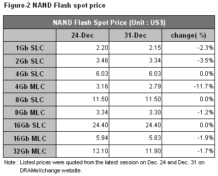
NAND Flash spot price recaps for Dec 24-31
In the SLC segment, 4Gb, 8Gb and 16Gb part managed to maintain price flat at US$6.03, US$11.50 and US$24.40 on a weekly basis, where downhill price trend was seen in other density of SLC chips. Price of 1Gb dropped by 2.3% to US$2.15 and 2Gb 3.5% to US$3.34. In the MLC segment, price drop maintained at single-digit percentage for most density of chips, except for 4Gb. Price of 4Gb dropped by 11.7% to US$2.79; 8Gb 1.2% to US$3.30; 16Gb 1.9% to US$5.83 and 32Gb 1.7% to US$11.90.